Information contained in the news release is current as of the date of announcement.
It is subject to change without prior notice.
Pioneer Develops High Efficiency Electro-Emission Device
"HEED" (Negishi Effect)

March 17, 1997 --- Tokyo, Japan, Pioneer Electronic Corporation announced the development of High Efficiency Electro-Emission Device "HEED" (Negishi Effect).
HEED has achieved an extraordinary electro-emission efficiency of 30% (conventional figure : under 1% ), which will be applicable to the hypothetical next generation flat panel display, and to the age of high-speed micro electronic necessary to vacuum micro electronic devices*.
Pioneer plans to develop this new technology for future business ventures.
As a solution to a hypothetical next generation flat panel display and/or for a future vacuum micro electronic device, providing a switching speed of over 100GHz(Giga : 1 billion) which cannot be achieved by semi-conductors,development of reliable and high performance cold cathodes is currently being pursued around the world. Various methods such as field emitting cathodes known as field emission display (FED), cathodes having diode structure represented by metal-insulator-metal (MIM), and metal-insulator- semiconductor (MIS) types have been tried previously. Among them the diode structured cathode is the most promising as a high performance cold cathode because it does not require a special high vacuum working environment. However, the electro-emission efficiency of such devices barely reachs 1 %. The emission efficiency is the ratio of the emitting current to the diode current which passes through an insulating film. This low efficiency makes it difficult to put this technology into practical use.
We have achieved this time an extraordinary rate of efficiency using the cathode in the MIS diode structure. This has been realized by providing an amorphous silicon oxide(SiOx) employing our original thin film deposition process between the silicon(Si) thin film and an ultra thin electrode made of platinum(Pt).
By applying a voltage of about 60 volts between an aluminum (Al) electrode and a Pt electrode, electrons start emitting from the Pt electrode surface. Further augmenting this voltage, electron emission grows at an accelerated pace, and at 90 volts we get a very large emission current density of 1.8 mA/cm2 which corresponds to an electro-emission efficiency of 30 %.
The MIS diode structure studied previously typically consists of an insulator of a very thin homogeneous film of less than ten nanometers (nano : 1/1 billion) thickness under which the tunneling effect takes place and that does not exhibit dielectric breakdown. Such a thin insulator film is difficult to manufacture especially for larger areas. In contrast to previous research, the insulator film Pioneer has developed is a thick SiOx of a several to several hundred nanometers, formally unthinkable in its theory, which results in high electro-emission and efficiency. (Using the inventor's name, we call this the "Negishi Effect".)
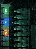
When these flatbed-electron emitting sources are applied to a flat panel display making use of fluorescent materials found in a conventional CRT tube, a high brightness of 80,000 cd/m2 has been obtained with the application of 90 volts and the accelerating voltage of 5 kV.
Search for Other resources
Search for Keyword
Search by date


= A device which uses the characteristics of the cold cathode (=a cathode which emits electrons in a vaccum environment with the application of a high electronic field without the use of external heat) to emit electrons in an high vaccum environment.